Jacob Trevino, PhD New York, NY
Build the lab.Ship the device.Grow the network.
As Senior Director of Columbia’s shared cleanroom, imaging, and characterization labs, Chief Innovation Officer at Chemeleon, and founder of Nanotech NYC, my work spans three worlds: directing advanced research facilities, commercializing point-of-need optical sensor hardware, and convening the region’s deep-tech ecosystem. Physics, hardware, and the communities that bring them to life.
Three disciplines, one through‑line.
Scaling physical infrastructure, commercializing nanoscale science, and cultivating community: each discipline reinforces the other two.
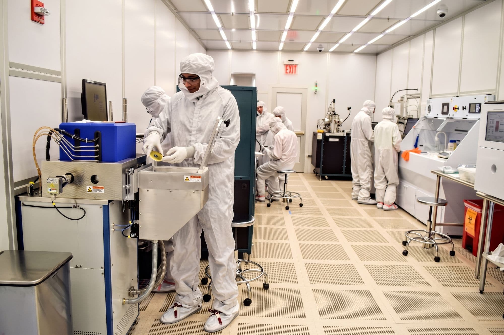
Cleanrooms are living systems. I design, modernize, and scale them.
From building CUNY ASRC’s nanofabrication facility from the ground up to directing and modernizing shared labs at NYU Tandon, Penn’s Quattrone Nanofab, and Columbia’s Nano Initiative, I turn complex physical infrastructure into thriving research engines. My playbook centers on scalability: digital operations, rigorous safety and training workflows, sustainable rate structures, and open-access ecosystems that connect academic and industry innovators.
Numbers with receipts.
The scale of the labs, awards, publications and community behind the work.
4
University shared labs led
CUNY ASRC, NYU Tandon, Penn Quattrone Nanofab and Columbia Nano Initiative
$17.5M
Cleanroom design & build
Supervised with contractors, architects and consultants — CUNY ASRC
$12M
Equipment stood up
Selected, acquired and installed across the labs I've led
40+
Ecosystem meetups hosted
In-person Nanonite socials and community gatherings convened across the New York region
$3.76M
External awards
NIH, NSF and NYC EDC — as PI, co-PI or senior personnel
37
Papers, chapters & patent filings
25 papers, 6 book chapters and 6 published patent applications
Twenty years, one stack.
From MEMS process engineering to research infrastructure to a startup and a community. Filter by track, or open any role for detail.
- Visit Columbia Univ. (opens in a new tab)
Senior Director, CNI Shared Labs
Jul 2025 – Present
- Provide strategic leadership and operational oversight for Columbia’s shared cleanroom, imaging, and materials characterization laboratories under the Columbia Nano Initiative.
- Manage interdisciplinary research infrastructure supporting faculty, students, and external collaborators across engineering, physical sciences, and biomedical fields.
- Coordinate compliance, safety, and training programs in alignment with university policies and federal regulations governing shared research facilities.
Chief Innovation Officer
Jun 2024 – Present
- Lead the development and implementation of innovative strategies to drive the company’s growth and competitive edge.
- Oversee R&D initiatives and manage the innovation pipeline from idea generation through commercialization.
- Develop and manage partnerships with academic institutions, industry leaders, and research organizations.
- Spearhead proposals for grants and funding opportunities (NSF, NIH, DoD) for new product development.
Chief Executive Officer
May 2022 – Jun 2024
- Directed overall operations, strategy and procedures across business development, market research, finance, operations and marketing.
- Developed a strategic roadmap for scaling prototype devices to foundry-level manufacturing.
- Raised funding through investor relations, venture capital, and grant proposals; built relationships with investors, partners and stakeholders.
Visit Chemeleon (opens in a new tab)Principal Scientist
Mar 2018 – May 2022
- Designed, simulated, fabricated, and tested next-generation colorimetric chemical sensors.
- Combined nanotechnology, photonics, and molecular recognition to create devices for commercial, medical, environmental, and food industries.
- Developed and wrote SBIR proposals (NSF, NIH, DoD), including the NIH SBIR Phase I and II awards for a cerebrospinal-fluid leak sensor.
Passing it on.
The work only compounds if people can learn it, borrow it and build on it. Four ways I try to make that happen.

Teaching
Abstract ideas, made concrete.
Make students think like scientists while learning their course materials: motivate abstract ideas with real applications, connect each new concept to what came before, and keep the big picture in view.
Principles of Device Microfabrication
Columbia University · School of Engineering
Diffusion, ion implantation, lithography and etching, with applications across biomedical, energy and photonics industries.
Graduate · 2015 – 2024
Microfluidic Devices in Biotechnology
City College of New York · Biomedical Engineering
Fundamentals, electrophoresis and flow cytometry, with hands-on fabrication in the ASRC NanoFabrication Facility.
Graduate & undergraduate · Fall 2016, 2017
Lab Techniques for Research in Nanotechnology & Materials Chemistry
The Graduate Center, CUNY
Biomolecular nanotechnology, nanophotonics and microscopy, with group fabrication projects.
Graduate · Spring 2016, 2017
Mentoring
“Easily the most rewarding and meaningful thing I choose to spend my professional time on.”
- The Bridge Golf Foundation (opens in a new tab)After-school mentor — a consistent source of support in academics, sports and life.
- NYAS Mentor Program (opens in a new tab)Mentoring early-career scientists since 2019.
- Undergraduate researchSummer nanotechnology and photonics research students at CUNY ASRC; engagement with Susquehanna University alumni.
- Materials Research SocietyCo-founded chapters at Boston University and CUNY; faculty advisor at CUNY; academic affairs committee member.
Science communication
Explain it clearly, or it doesn’t count.
Scientists collect and generate the data everyone else depends on. That comes with a responsibility to explain it — clearly, honestly, and to audiences that aren’t already convinced.
The best moment in any talk is watching squinting confusion turn into understanding. Nanotech NYC exists partly to amplify other researchers’ work in exactly that way.
Invite me to speakAdvisory
Scientific and digital consulting.
- Micro- and nanofabrication process development
- Nanophotonic systems design & fabrication
- MEMS manufacturing
- Nanomaterials
- Shared-lab and cleanroom strategy
Digital consulting for startups, academic labs and small businesses: websites, branding, analytics, SEO and content strategy.
Start a conversationThe record.
Two decades across nanophotonics, plasmonics and MEMS — from Vogel spirals and silicon-carbide packaging to colorimetric-sensor patent applications.
10 selected of 37
2026
Open Devices and methods for detecting and quantifying a target analyte of interest (opens in a new tab)Devices and methods for detecting and quantifying a target analyte of interest
J. Trevino et al.
US 2026/0104410 A1 · Chemeleon Inc., Published application · filed Oct 15, 2025 · priority Oct 15, 2024
- Patent application
- Sensing & diagnostics
2024
Open Clickable and cleavable sensing surface and method of making the same (opens in a new tab)Clickable and cleavable sensing surface and method of making the same
J. Trevino et al.
US 2024/0125778 A1 · DrinkSavvy, Inc. (dba Chemeleon), Published application · filed Oct 16, 2023 · priority Oct 14, 2022
- Patent application
- Sensing & diagnostics
2024
Open Integrated molecular sensor device and method for making same (opens in a new tab)Integrated molecular sensor device and method for making same
J. Trevino et al.
US 2024/0068018 A1 · DrinkSavvy, Inc., Published application · filed Aug 25, 2023 · priority Aug 26, 2022
- Patent application
- Sensing & diagnostics
2023
Open Devices and methods for detecting a target analyte of interest (opens in a new tab)Devices and methods for detecting a target analyte of interest
J. Trevino et al.
US 2023/0296614 A1 · DrinkSavvy, Inc. (dba Chemeleon), Published application · filed Aug 3, 2021 · priority Aug 3, 2020
- Patent application
- Sensing & diagnostics
2021
Find Purcell Effect of Plasmonic Surface Lattice Resonances and Its Influence on Energy Transfer (opens in a new tab)Purcell Effect of Plasmonic Surface Lattice Resonances and Its Influence on Energy Transfer
R. Collison, J.B. Pérez-Sánchez, M. Du, J. Trevino, J. Yuen-Zhou, S. O’Brien, V. Menon
ACS Photonics, 8(8), 2211–2219
- Paper
- Nanophotonics
2018
Find Long-Range Self-Assembly via the Mutual Lorentz Force of Plasmon Radiation (opens in a new tab)Long-Range Self-Assembly via the Mutual Lorentz Force of Plasmon Radiation
H. Ji, J. Trevino, R. Tu, E. Knapp, J. McQuade, V. Yurkiv, F. Mashayek, LT. Vuong
Nano Letters, 18(4), 2564–2570
- Paper
- Nanophotonics
- Materials & assembly
2014
Find Doped polycrystalline 3C-SiC films with low stress for MEMS: part I — Deposition conditions and film properties (opens in a new tab)Doped polycrystalline 3C-SiC films with low stress for MEMS: part I — Deposition conditions and film properties
X.A. Fu, J. Trevino, M. Mehregany, C.A. Zorman
J. Micromechanics and Microengineering, 24(3), 035013
- Paper
- MEMS
- Materials & assembly
2012
Find Geometrical structure, multifractal spectra and localized optical modes of aperiodic Vogel spirals (opens in a new tab)Geometrical structure, multifractal spectra and localized optical modes of aperiodic Vogel spirals
J. Trevino, S.F. Liew, H. Noh, H. Cao, L. Dal Negro
Optics Express, 20(3), 3015–3033
- Paper
- Nanophotonics
2011
Find Circularly-symmetric light scattering from nanoplasmonic spirals (opens in a new tab)Circularly-symmetric light scattering from nanoplasmonic spirals
J. Trevino, H. Cao, L. Dal Negro
Nano Letters, 11(5), 2008
- Paper
- Nanophotonics
2006
Find An all-glass chip-scale MEMS package with variable cavity pressure (opens in a new tab)An all-glass chip-scale MEMS package with variable cavity pressure
D. Sparks, J. Trevino, S. Massoud-Ansari, N. Najafi
J. Micromechanics and Microengineering, 16, 2488–2491
- Paper
- MEMS
Invite me to speak.
Keynotes, panels, guest lectures and workshops for research, industry and community audiences.
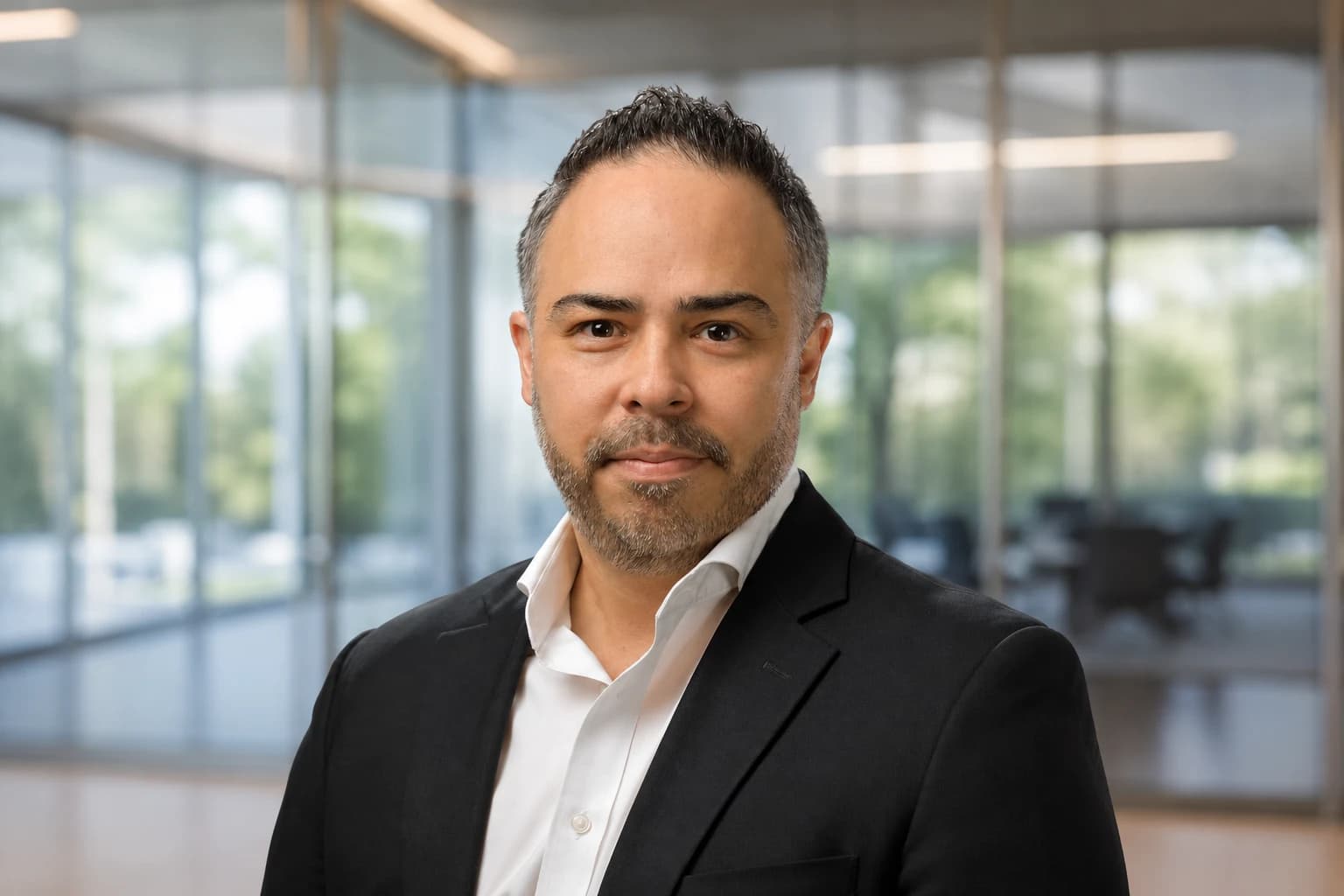
Talk topics
- 01
Running a shared cleanroom like a product
What it takes to design, staff and grow research infrastructure that researchers actually choose to use.
- 02
From SBIR to foundry: taking a sensor out of the lab
Lessons from taking a nanophotonic colorimetric sensor from bench prototype to a fundable, manufacturable product.
- 03
Building a regional deep-tech community from zero
The Nanotech NYC playbook: directories, meetups, Slack, and consortia like MANTH.
- 04
Light, order and the Vogel spiral
A tour of aperiodic nanophotonics for curious non-physicists — how structure without repetition controls light.
- 05
Science communication for scientists
Why explaining your work to non-experts is part of the job, and how to do it without dumbing it down.
Have a different angle in mind? Most of these adapt well to the audience — tell me about yours.
Let’s build something.
Advisory work, speaking invitations, research partnerships, or lab and facility strategy. Tell me what you’re working on and where I might help.